Semiconductor Packaging Material Market Analysis and Overview
Market Research Future Insights:
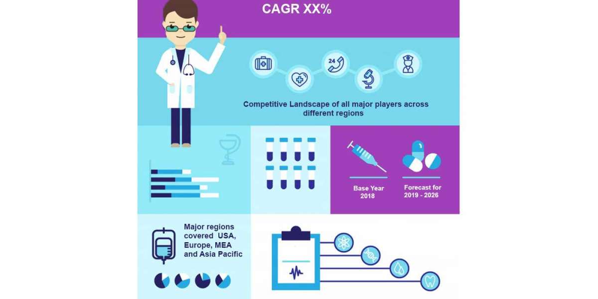
The Semiconductor Packaging Material Market has reached the value of USD 28,150 million in 2030 and due to the demand, it is estimated to reach at a CAGR of 8.30% by 2030.
Materials for semiconductor packaging are helpful when fabricating semiconductor devices. They are employed to protect equipment against deterioration and outside impact.
The sharpening miniaturisation of electronic devices is a factor that will affect the global market for semiconductor packaging materials. Other significant drivers of market expansion include the steadily expanding mobile industry, rising demand for mobile and communication devices, expanding use of integrated circuits in a variety of electronic devices, rapid technological advancements, a shift in consumer preferences toward modern electronics, and rising demand for compact devices across a range of industries.
Get free sample report @ https://www.marketresearchfuture.com/sample_request/1217
Key Players:
The major participants in the world market for semiconductor packaging materials are Alent PLC (UK), Alpha Advanced Materials (USA), BASF SE (Germany), E. I. du Pont de Nemours and Company (USA), Henkel AG Company, KGaA (Germany), Hitachi Chemical Company, Ltd. (Japan), Honeywell International Inc. (USA), Kyocera Chemical Corporation (Japan), LG Chem (South Korea), Mitsui High-tec, Inc.
Regional Analysis :
The global market for semiconductor packaging materials is divided into four regional markets: Europe, North America, Asia Pacific, and the Middle East and Africa (MEA). The semiconductor packaging material market is currently led by the Asia Pacific region, and during the anticipated period, this trend is likely to continue as a result of the region's rapid technological development and growing consumer demand for advanced electronic packaging materials. At the same time, significant investments in electronics applications, simple accessibility to raw materials, affordable manufacturing, and a cheap labour force are driving market expansion in this area. Australia, China, India, Japan, and South Korea are the leading national markets in this region, followed by the remaining nations in the Asia Pacific.
Due to technological advancement, a variety of established industries, and the presence of numerous important market players, North America is another crucial regional market. The USA and Canada are the two most important national markets in this area.
Similar to North America, Europe is a significant regional market that is expanding. France, Germany, Spain, and the United Kingdom are the major national markets in this area, followed by the rest of Europe. Due to its impoverished nations, lack of awareness, education, infrastructure, and technological advancement, the MEA region has a small regional market.
Browse Complete Report @ https://www.marketresearchfuture.com/reports/semiconductor-packaging-material-market-1217
Market Segmentation :
Technology, type, and finally geography have all been used to segment the global market for semiconductor packaging materials. The dual in-line package, dual flat no-leads, grid array, quad flat package, tiny outline package, and other technologies are included in the technology-based market segmentation. Grid array is anticipated to experience the quickest growth during the forecast period due to its widespread adoption across all significant semiconductor packaging types.
Bonding wires, ceramic packages, encapsulation resins, organic substrates, solder balls, wafer level packaging dielectrics, and other products have all been categorised into types of market segments. Due to their capacity to serve as the foundation layers of single semiconductor devices and chips, on which additional layers can be deposited to complete the circuit, organic substrates are anticipated to dominate the market during the forecast period.
Human Machine Interface (HMI) Market to Reach USD 9,652.6 Million by 2030, at a CAGR of 9.1% - Market Research Future (MRFR)
GaN Semiconductor Devices Market is Anticipated to reach USD 29.6 Billion by 2030, at a 5.8% of CAGR - Market Research Future (MRFR)
Underwater Robotics Market to Reach USD 5.003 Billion, at a 12.50% CAGR By 2030 - Market Research Future (MRFR)
Broadcasting Equipment Market Valued at USD 407.9 billion, at a 6.10% CAGR By 2032 - Market Research Future (MRFR)
SerDes Market to Reach USD 1.3 Billion, at a 15.2% CAGR By 2030 - Market Research Future (MRFR)